+


S5600 PCI-EXPRESS PCI-E PCIE X4 FPGA Development Board PCIE Development Board winder
new features:
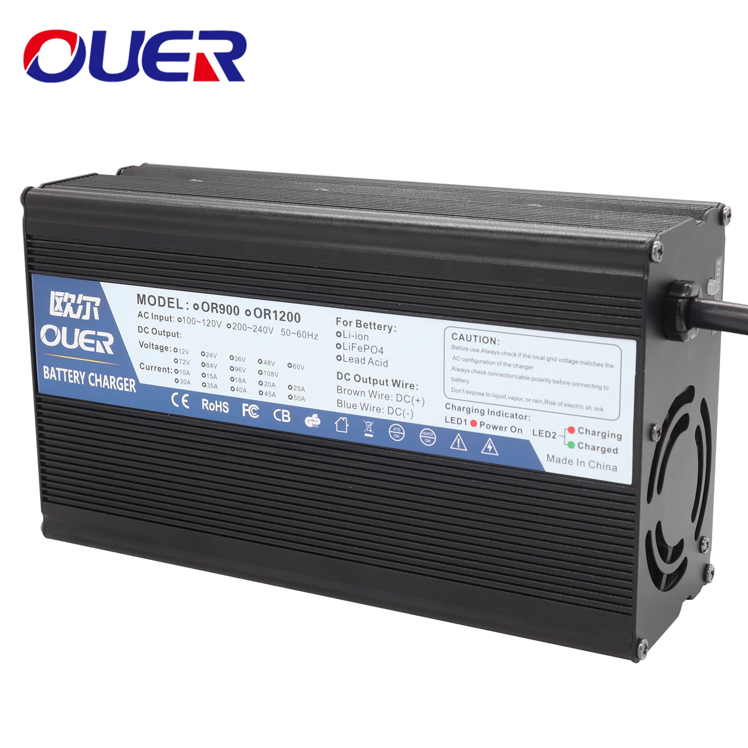
S5600PCI-EX4 development platform main hardware specifications:FPGA: EP4CGX30CF23C8 (optional EP4CGX50CF23, EP4CGX75CF23, pin is fully compatible), the device speed is also optional -6, -7 high-speed devices. FPGA provides PCI-E HARD IP, to achieve the PCI-E protocol 1.1 physical layer and data link layer protocol, users only need to design PCI-E protocol TLP (data transport layer) and application layer, simplifying the user's design. PCI-E physical layer and data link layer by the HARD IP implementation, does not take up FPGA resources, stable and reliable.DDR2 SDRAM DIMM module: standard 200-pin DDR2 SDRAM notebook memory module, can provide 1G, 2G (standard configuration), 4G bytes of memory capacity, can achieve 133 (device speed -8) / 166 (device speed -7) / 200 (device speed -6) MHz clock frequency, can achieve the lowest 2.13G bytes / sec burst read and write speed.80 USER GPIO input and output: support IO voltage 3.3V, 2.5V, 1.8V and 1.5V, support LVDS input and output.JTAG and AS download port: support QUARTUS online debugging and compilation download function, EPCS16 configuration device to meet the EP4CGX70 configuration requirements.
S5600PCI-EX4 development platform Main software specifications:PCI-EX4 HARD IP: implemented by FPGA internal hardware, does not occupy FPGA resources, to achieve the PCI-E protocol physical layer and data link layer, stable and reliable, the data transmission layer and application layer interface using AVALON ST interface.PCI-E data transmission layer: complete VHDL source code design, to achieve the PCI-E protocol data transmission layer (TLP layer), support memory read, memory write, DMA memory read, DMA memory write, DMA memory read complete, memory read Completion of several TLP packet format, PAYLOAD data load size support 4 to 256 bytes automatically variable, the interface using AVALON ST interface, directly connected to the FPGA PCI-E HARD IP interface.User application layer: complete VHDL source code design, support 64-bit FIFO input and output interface, 32-bit SLAVE memory mapped read and write interface, support for external interrupt input.DDR2 memory read and write interface: complete VHDL source code design, control data input and output to the ALTERA standard DD2 SDRAM IP, to achieve data transfer and cache function.Drivers and test programs: Driver and application development platform using VC6 development platform, DDK development tools to support, drivers and applications complete source code design, support DMA read and write, memory mapping read and write, interrupt input function. The driver supports DMA read and write performance test, DMA data validation test and data storage file function. Drive and test procedures using WDM driver structure, support WIN2000, XP, WIN7 and other operating systems.
S5600 PCI-E high-speed data development platform internal port block diagram is as follows:
The S5600 PCI-EXPRESSX4 development platform suite includes the following:S5600 PCI-E x4 development platform hardware circuit board one;2G bytes DDR2 SDRAM notebook memory one;ALTERA BYTEBLASTER2 download line one;ALTERA QUARTUS2 11.0 development platform installation CD;DDK and DRIVERWORKS driver development tools CD;FPGA internal source code design and use manual and description;Driver complete source code design and use manual and description;S5600 circuit schematic and PCB design;
Performance and compatibility, stability testingThe PCI-E development board is tested on the following PC-compatible and powered on normally:Performance test using the maximum cycle of transmission, each DMA block size of 512K bytes, according to the average flow of 60 seconds, calculated by the number of seconds to transfer the number of DMA block calculation. Impact of PCI-E performance In addition to DMA block size, PCI-E PAYLOAD (data load) also affect the read and write performance. General PC chipset support 128 bytes of DMA read and write PAYLOAD, 128 bytes of PAYLOAD DMA read and write utilization rate of 82%, a small number of PC chipset support 256 bytes of DMA read and write PAYLOAD, you can open inside the CMOS, Improve read and write performance, 256 bytes of PAYLOAD DMA read and write utilization rate of 91%.DMA data load is 128 bytes of performance:CPU operating system DMA read (host memory to card) DMA write (card to host memory)CORE-I3 XP 523M bytes / sec 752M bytes / secondCORE E7200 XP 508M bytes / sec 746M bytes / second
DMA data load is 256 bytes of performance:CPU operating system DMA read (host memory to card) DMA write (card to host memory)CORE-I3 XP 592M bytes / sec 836M bytes / secondAMD965 XP 511M bytes / sec 822M bytes / sec
S5600 PCI-EX4 development platform Application:Industrial data acquisition, a / d, d / a data transformation, data processingHigh-speed high-resolution video data acquisition, 1080P real-time video capture display;High - speed data buffering, high - speed data encryptionHigh speed industrial control;

http://www.mbm-chip.com
Origin : Mainland China